Glass & substrate science
Glass Surface Roughness and Scattering: How a Few Nanometres of Ra Affect the Transmission Signal

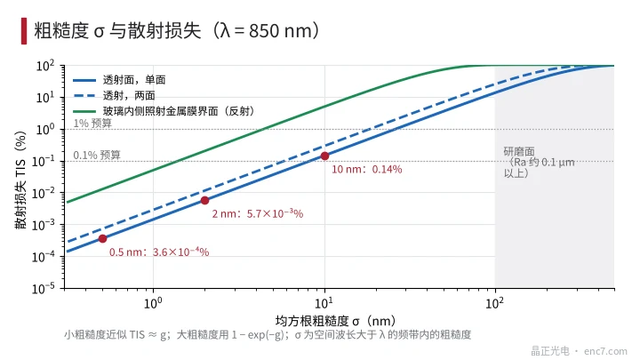
Total integrated scatter of a transmitting surface is TIS ≈ (2π(n−1)σ/λ)²: at 850 nm, σ = 0.5, 2 and 10 nm give single-face TIS of only 0.00036%, 0.0057% and 0.14%. This article gives an angular-distribution model, compares sensitivity of phase gratings, coatings and reflecting interfaces, and backs out polish grade from a scatter budget.
Polish requirements for glass substrates are often written “Ra ≤ a few nanometres”, and price rises steeply with grade. Yet encoder readout light is at 850 nm — how much light does a few-nanometre surface undulation actually remove from the transmission signal, and where does that light go? This article computes scatter loss and angular distribution with a phase-screen model, then asks which process steps truly need super-smooth surfaces, and finally shows how to back out roughness from a scatter budget.
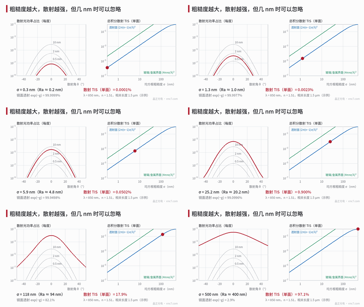
Model: surface height becomes phase
Light leaving glass (index n) into air gains an optical-path difference (n−1)·h for every surface-height difference h. The variance of the phase fluctuation is
g = [2π(n − 1)σ / λ]²
where σ is rms surface roughness and λ the wavelength. Specular transmitted light decays by coherent superposition as exp(−g); the remainder is scattered, and total integrated scatter is
TIS = 1 − exp(−g) ≈ g(g ≪ 1)
For a reflecting interface — e.g. light from inside the glass onto a metal film — the path difference is 2nh and TIS ≈ (4πnσ/λ)². The phase coefficient is 2n/(n−1) ≈ 6 times that of a transmitting face, so TIS is about 35 times larger; reflecting surfaces are far more roughness-sensitive.
Angular distribution of scattered light is set by the correlation length ℓ. For Gaussian correlation and g ≪ 1 the diffuse scatter approximates exp[−(πℓ·sinθ/λ)²]: at ℓ = 1.5 μm, λ = 0.85 μm the 1/e half-width is about 10°, shape independent of σ; σ only scales the overall height. Only when g approaches 1 (ground surfaces with σ about 100–300 nm) does the pattern broaden markedly and the specular part vanish quickly (Figure 1, right half). Here σ is roughness in the spatial-wavelength band longer than λ; AFM small-field scans and optical-profiler σ are not directly interchangeable.
Worked example: 0.5, 2 and 10 nm
At λ = 850 nm, n = 1.51, σ maps to scatter as follows (Ra taken as 0.8σ for a Gaussian surface):
| σ (nm) | Ra (nm) | Single-face TIS | Two-face TIS | Glass/metal interface TIS |
|---|---|---|---|---|
| 0.5 | 0.4 | 0.00036% | 0.00071% | 0.012% |
| 2 | 1.6 | 0.0057% | 0.011% | 0.20% |
| 10 | 8 | 0.14% | 0.28% | 4.9% |
| 20 | 16 | 0.57% | 1.1% | 18% |
| 50 | 40 | 3.5% | 6.9% | 71% |
| 100 | 80 | 13% | 25% | 99% |
| 300 | 240 | 72% | 92% | nearly all |
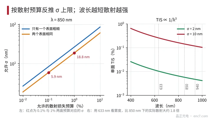
TIS scales with σ²: every 3× rise in σ multiplies scatter by nearly 10; it scales inversely with λ², so haze viewed at 633 nm is about 1.8× the actual scatter at 850 nm (Figure 3, right). Below 10 nm the effect on the transmission signal is far smaller than Fresnel reflection of the glass (about 8% for two faces); scattered light also concentrates within about ±10° (this example correlation length), and if the readhead acceptance angle is larger the real loss is even smaller.
Which steps are roughness-sensitive
Amplitude-type transmission readout. Opaque/clear contrast comes from the chrome film; roughness causes only sub-percent overall attenuation, bright and dark states scale together, and modulation is unchanged. A few nanometres versus a few tenths of a nanometre make no signal difference.
Phase grating. π phase depth d = λ/(2(n−1)) ≈ 833 nm; at σ = 10 nm the roughness-induced phase error 2π(n−1)σ/λ ≈ 0.038 rad and the zero-order increase is about g/4 ≈ 3.6×10⁻⁴ — negligible; but 0.14% of scatter background adds directly to zero order and stray light. If the combined zero-order-plus-stray budget is set at 1% (example), that already takes more than a tenth of it.
Coated faces and reflecting interfaces. Chrome is about 100 nm thick; a σ = 10 nm undulation is one tenth of film thickness, so local thickness and OD fluctuate with it. Illuminating a metal film from inside the glass, 10 nm already scatters about 5% of the light; a 1% budget allows only σ ≈ 4.5 nm, a 0.1% budget about 1.4 nm.
Contact exposure. Peak-to-valley for σ = 10 nm is about 50 nm; diffraction blur from the contact gap is about √(λ_expo·g) ≈ 0.14 μm (λ_expo = 365 nm, g = 50 nm), far below encoder line width. What limits exposure quality is flatness and particles, not nanometre-class roughness.
Defects rms cannot describe. Scratches, digs and subsurface cracks are local defects; σ can be small yet they can be numerous. They are the sources of pinholes, broken lines and coating peel — polish grade must also state a surface-imperfection grade.
Backing out σ from a scatter budget
Given an allowed scatter budget B and two identical faces,
σ_max = λ / [2π(n − 1)] · √[−ln(1 − B) / 2]
At B = 0.1%, σ_max ≈ 5.9 nm (Ra about 4.7 nm); at B = 1% about 18.8 nm (Ra about 15 nm); with only one rough face the limits are 8.4 nm and 26.6 nm (Figure 3, left).
Engineering notes
- For the optical faces of amplitude-type transmission discs, σ ≤ 20 nm (Ra about 15 nm, two-face TIS about 1%) is enough; chasing Ra < 1 nm gains nothing for the signal.
- For phase gratings, interferometric readout or high-precision coating faces, take σ ≤ 2–5 nm and also limit scratch/dig grade.
- Reflecting structures (metal film lit from inside the glass) allow only about one sixth the σ of a transmitting face — budget separately.
- OD, ID and non-optical faces may be ground; polish is unnecessary. As-drawn float surfaces are already sub-nanometre to about 1 nm class.
- Roughness acceptance must state method, field of view and filter bandwidth; visual haze at 633 nm overestimates scatter at 850 nm.
- Ground surfaces (Ra 0.1 μm and above) on an optical path scatter more than a tenth of the light on one face alone — polish before use.
Summary
Scatter loss of a transmitting face scales with σ² and inversely with λ²: below 10 nm at 850 nm, single-face loss stays within 0.14% and is negligible for amplitude-type disc signals. Super-smooth surfaces are truly needed for phase gratings, reflecting interfaces and high-precision coatings, together with control of local defects such as scratches and digs. Polish grade should be set by scatter budget and process step — not by chasing the highest grade across the board.
Translated from the ENC7 Chinese technical library (article 0574). Read the Chinese original. Need a disc built to your drawing? Request a quote or see our custom encoder discs.
© Langfang Jingzheng Optoelectronic Technology Co., Ltd. All rights reserved. This article was created with AI assistance.