Troubleshooting
Troubleshooting: Lissajous Circle Off Centre — Sources of DC Offset and How to Find Them
A Lissajous circle whose centre is offset from the origin indicates DC offset. A relative offset ε produces an error once per period of about ε rad — about 1″ per 1% at 2,048 lines. This article derives ε = κ/M, illumination asymmetry amplified by the modulation, analyses when duty cycle, stray light and dark current matter, and gives a step-by-step measurement method and a criteria table.
In oscilloscope X-Y mode with DC coupling, the Lissajous circle has normal size and shape but its centre is not at the origin; it is shifted to one side. This is DC offset: A or B carries a constant that does not change with position. The interpolation error it causes occurs once per signal period and is conspicuous at high interpolation factors. This article first gives how to read ε and the resulting error, then analyses the sources and magnitudes of offset one by one, and finally gives a step-by-step measurement method and criteria.
Error and how to read ε
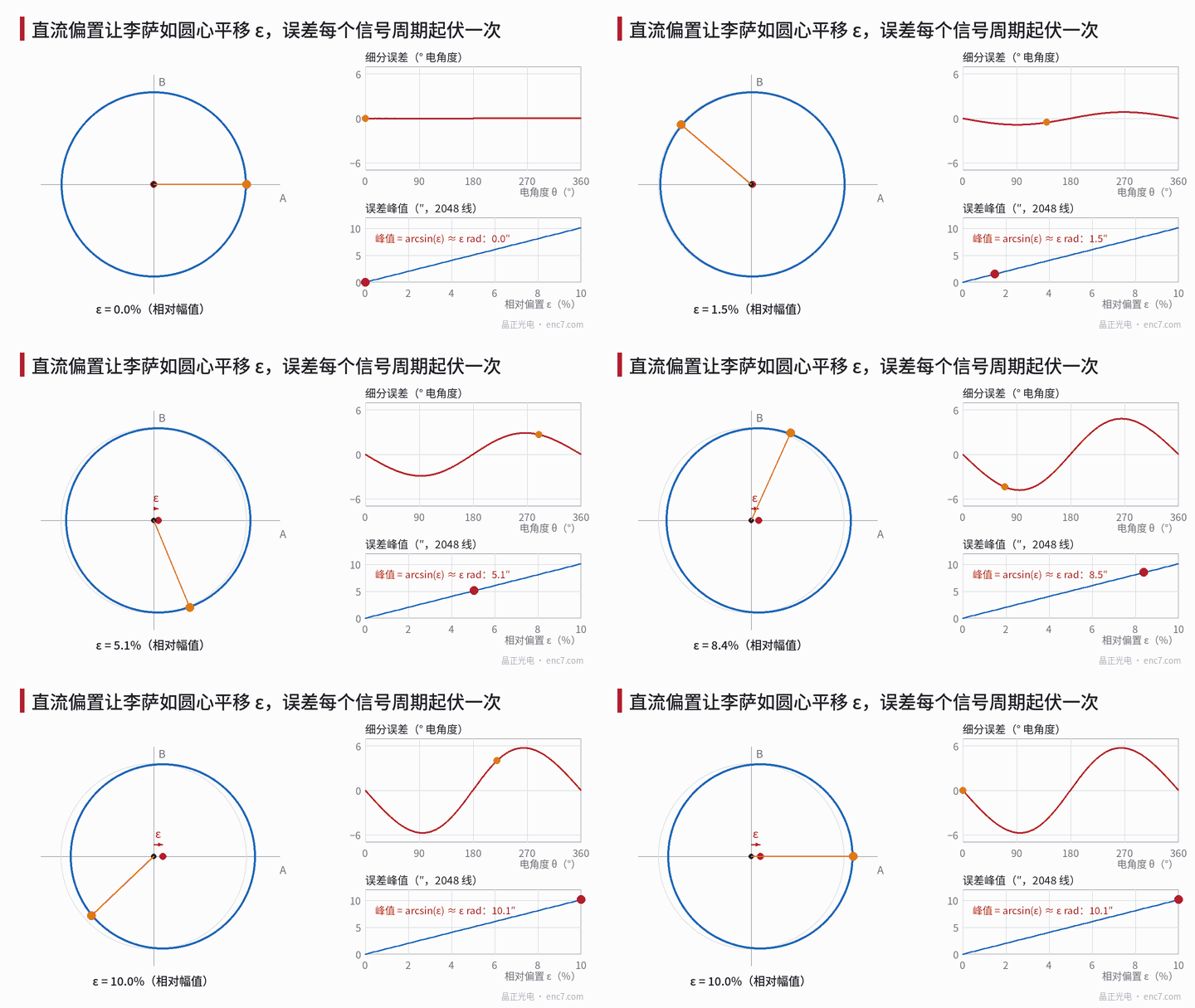
For channel A, let A = a·cosθ + o_A. Read the maximum and minimum from the Lissajous figure or the single-channel waveform:
ε_A = o_A/a = (X_max + X_min)/(X_max − X_min)
Likewise for B. With A = cosθ + ε, the atan2 error occurs once per period with peak exactly arcsin(ε), about ε rad for small values; with offset on both channels the peak is about √(ε_A² + ε_B²). At 2,048 lines, 1% offset is about 1.0″.
Use DC coupling when measuring; for differential signals use a differential probe or measure A+ and A− separately and subtract. AC coupling filters the offset out, and the centre always appears to be at the origin.
Sources and magnitudes
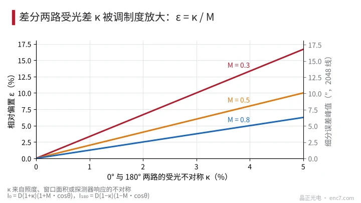
Illumination asymmetry between the two differential channels. A = I₀ − I₁₈₀. Suppose the DC of the two channels differs by ±κ because of illumination, window area or detector response:
I₀ = D·(1 + κ)·(1 + M·cosθ), I₁₈₀ = D·(1 − κ)·(1 − M·cosθ)
Subtracting gives A = 2κD + 2DM·cosθ, so
ε = κ / M
where D is each channel’s DC and M the modulation. Differential operation is meant to cancel DC, but it only cancels the part common to both channels; the remaining asymmetry is amplified by 1/M. With κ = 1% and M = 0.5, ε = 2%, about 2.0″ at 2,048 lines; with M down to 0.3, the same κ becomes 3.3% (Figure 2). On the disc side, κ comes from different transmittance of the clear areas under the two detection fields — e.g. residual film, haze or stains falling on only one channel; the quantitative model for local contamination is in the library article on contamination.
Transmitting-to-opaque area ratio. When the 0° and 180° channels come from the same track with identical windows, the average transmittance each sees is the disc duty cycle D_c times the window duty cycle; their DC is strictly identical, and duty-cycle deviation produces no offset. But if a fixed reference level or a separate reference photodiode replaces the inverted channel, duty-cycle deviation becomes offset directly. With a 50% index window:
ε = (D_c − 0.5)·π² / (4·sin(πD_c))
At D_c = 0.45, ε ≈ −12.5% — quite large. So the same line-width deviation is harmless in a true differential design but the main error source in a reference-level design.
Stray and background light. Uniform background light reaches both channels and cancels in the difference; stray light reaching only one channel, at a fraction β of that channel’s DC, gives ε ≈ β/(2M). Hub edges, housing inner walls and chrome-surface reflections can all sweep just one channel; at M = 0.5, β = 2% already gives about 2% offset.
Dark current and circuit offset. A dark current difference ΔI_d between the channels gives ε = ΔI_d/(2M·I₀), where I₀ is each channel’s photocurrent; at room temperature it is generally negligible, but it roughly doubles every 8–10 °C at high temperature — see the library article on readhead temperature effects. Amplifier offset voltage referred to amplitude also appears as offset.
Step-by-step measurement: breaking the offset down
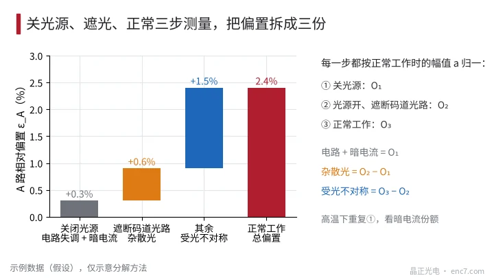
Three measurements, each normalised to the normal operating amplitude a, at the same angle and temperature:
- Light source off: read O₁, the sum of circuit offset and dark current.
- Light on, track light path blocked: insert an opaque sheet between the source and the track and read O₂; O₂ − O₁ is the contribution of stray light reaching the detector without passing the track.
- Normal operation: read O₃; O₃ − O₂ is illumination asymmetry (illumination, windows, detector response, local disc transmittance), and for reference-level designs also includes duty-cycle deviation.
Figure 3 shows a set of example data: total offset 2.4%, of which circuit and dark current 0.3%, stray light 0.6%, illumination asymmetry 1.5% — the priority is obvious. Note that step 2 also blocks reflections from the disc surface itself, which are counted in step 3. Two supplementary actions: repeat step 1 at high temperature to see if the dark-current share rises; repeat step 3 with a reference disc — if the step-3 result changes with the disc, the disc’s transmittance or duty cycle is at fault. If the circle centre also moves as the disc turns, the offset varies with angle, which is covered separately.
Criteria: allocate by accuracy class
Allowable offset is set by the error budget E (arcseconds) allocated to it:
ε_allow = sin(E·N/206265) ≈ E·N/206265
For square-wave outputs without interpolation, offset moves the comparator switching point by arcsin(ε) electrical, so the criterion becomes edge position. Example allocations:
| Use | Example requirement | Allowable offset ε |
|---|---|---|
| Square-wave x4 | Edge position error ≤ ±10° electrical | ≤ 17% |
| Square-wave x4 | Edge position error ≤ ±5° electrical | ≤ 8.7% |
| 2,048-line interpolation | 2″ allocated to offset | ≤ 2.0% |
| 2,048-line interpolation | 0.5″ allocated to offset | ≤ 0.5% |
| 5,000-line interpolation | 0.5″ allocated to offset | ≤ 1.2% |
| 10,000-line interpolation | 0.2″ allocated to offset | ≤ 1.0% |
Interpolation circuits with offset self-calibration can remove static offset, in which case the criterion governs post-calibration residual and drift; but too large an as-built offset uses up the correction range, so leave margin — e.g. as-built offset no more than half the correction range (example).
Engineering notes
- Use DC coupling and read ε as (X_max + X_min)/(X_max − X_min), reading each channel separately and then combining.
- Differential operation only cancels common DC; illumination asymmetry κ is amplified to κ/M. Raising modulation suppresses several offset sources at once.
- True differential designs are insensitive to disc duty-cycle deviation; reference-level designs are very sensitive — treat them differently in selection and incoming inspection.
- Evaluate stray light by whether it reaches only one channel; blacken hubs, clamp rings and housing inner surfaces, or keep them away from the read area.
- Use the three steps — source off, track path blocked, normal operation — to split offset into circuit, stray light and illumination asymmetry, then treat each.
- Allocate offset criteria by ε ≈ E·N/206265; the more lines, the larger the offset allowed for the same arcsecond budget.
Summary
An off-centre circle corresponds to DC offset, with error once per period of about ε rad. The main source is illumination asymmetry between the differential channels, amplified by modulation to κ/M; duty cycle only matters in reference-level designs; stray light and dark current matter when they act on one channel only. Step-by-step measurement breaks the total offset down, and the allowable value set by accuracy class decides whether it needs fixing.
Translated from the ENC7 Chinese technical library (article 0207). Read the Chinese original. Need a disc built to your drawing? Request a quote or see our custom encoder discs.
© Langfang Jingzheng Optoelectronic Technology Co., Ltd. All rights reserved. This article was created with AI assistance.